
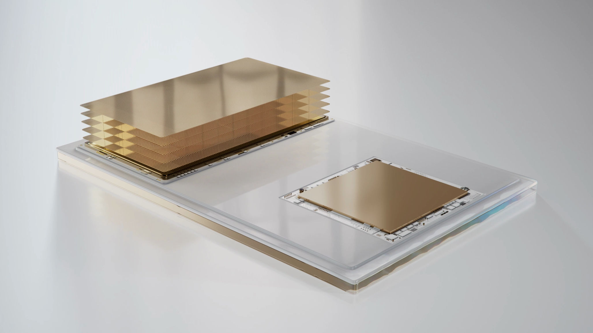
Qualcomm this morning is announcing that it has completed the initial validation of its High Bandwidth Compute (HBC) memory architecture, which will be a central part of the company’s upcoming Dragonfly data center AI accelerators. The stacked memory architecture will see Qualcomm and its manufacturing partners place multiple layers of DRAM on top of a small compute die in order to bring memory even closer to the compute hardware that is accessing it, allowing Qualcomm to reap the energy efficiency and cost efficiency benefits of a closer hardware placement.
The recent validation of the technology moves HBC one step closer to deployment in commercial products, which are scheduled to start sampling next year. Qualcomm has now validated that the technology works and is delivering energy efficiency and memory bandwidth close to their expectations, allowing them to move towards mass production next year while keeping customers (and investors) in the loop on the development of Qualcomm’s Dragonfly AI250 accelerator and its successors.
Qualcomm HBC: Near Memory Compute for Less Data Movement
First announced by Qualcomm back at their 2026 Investor Day, HBC is a new Qualcomm-spearheaded technology that is intending to use near-memory compute in order to strike a new balance between memory capacity, memory performance, and production costs – with Qualcomm looking to push the envelope on all three aspects.
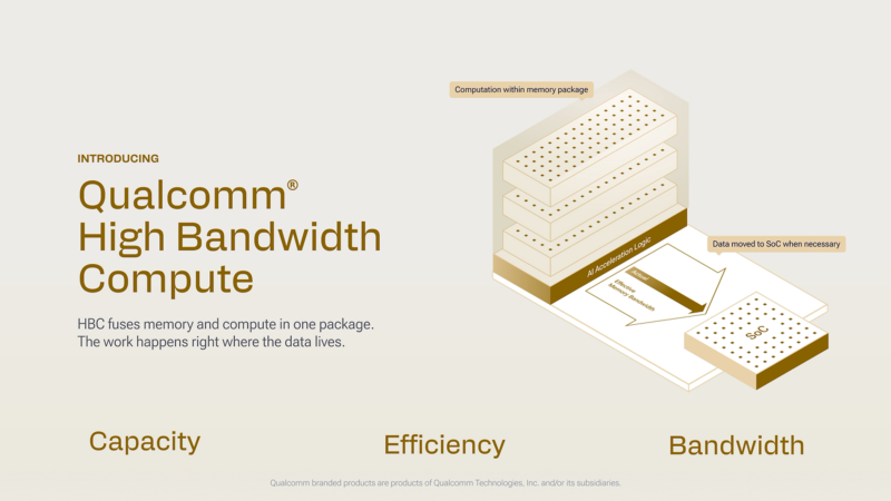
Fundamentally, the technology is a further variation on HBM and other memory stacking technologies. But unlike HBM where multiple DRAM dies are stacked on top of a base die that is connected back to the host processor over an ultra-wide memory bus, HBC aims to cut out the middleman by placing a small compute die at the bottom of the stack instead.
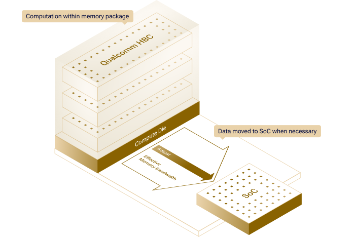
In principle, placing memory on top of a compute die has several benefits. The biggest of these is energy efficiency, as moving data around costs energy – and moving large amounts of data large distances costs even more energy. By placing memory on top of a compute die, this eliminates even the relatively short distance of an HBM connection (to say nothing of external memory like LPDDR5X), minimizing the amount of energy spent to move that data around. Those energy savings, in turn, can be funneled back into improving performance of the chip itself, or allowing a larger number of chips to be clustered together within the same energy footprint.
The compute die itself is not a full processor. But by placing the most memory bandwidth-intensive operations on the die and then sending the results from that back to the larger compute die at the center of the processor, Qualcomm is looking to get their memory and compute hardware as close together as is feasible.
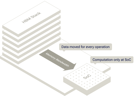
Qualcomm’s efforts are also eyeing production costs here. Because of the wide memory bus used by HBM, it required advanced packaging such as CoWoS or EMIB to connect HBM stacks to a compute die and memory controllers. But by shifting most of the computational workload to the compute die that sits under the memory, far less memory bandwidth is needed to connect the compute die to a larger processor die elsewhere on the chip package. And, consequently, that connection can be built with cheaper technologies such as traditional 2D organic substrates.
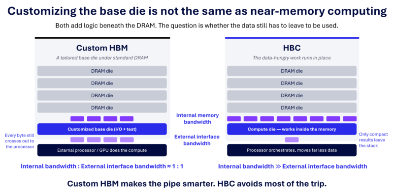
That said, HBC does not eliminate all of the complexity. Like HBM, it still requires bonding multiple DRAM dies (or in Qualcomm’s case: wafers) on top of another die using TSVs, which is itself a challenging process. Which means the need for complex manufacturing techniques has not gone away, but it has been reduced from both memory stacking and die-to-die connectivity to just the memory stacking.
Finally, Qualcomm is looking to strike a better balance between memory bandwidth and memory capacity here. Notably, the company’s HBC design calls for using LPDDR5X DRAM dies here rather than the thin, high-performance dies used by HBM. The company has not outlined what the final performance of the technology will be, but the capacity of an HBC stack is already projected to be larger than what current HBM4 implementations can achieve.
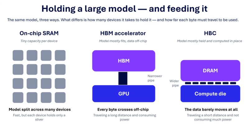
Qualcomm’s fundamental argument through all of this is that HBC provides a better all-around solution than any other memory architecture, be it HBM, on-die SRAM, or off-package LPDDR. As proposed, HBC has strengths and weaknesses versus all of these technologies, but as Qualcomm argues, they can achieve memory bandwidth (and thus performance) far better than external LPDDR – and approaching HBM – without the capacity constraints of using on-die SRAM, or the high costs of the latter of those two solutions.
Ultimately, all of this is meant to lead to allowing Qualcomm to build a better chip for AI inference, by meeting inference’s need for memory bandwidth and capacity with fewer drawbacks than existing technologies. It
Validating HBC: 2 Stack Test Finds 5x Bandwidth-per-Watt of HBM4
Diving into the validation process itself, for their initial HBC validation Qualcomm has hooked up an early HBC sample stack to a test unit in their San Diego labs.
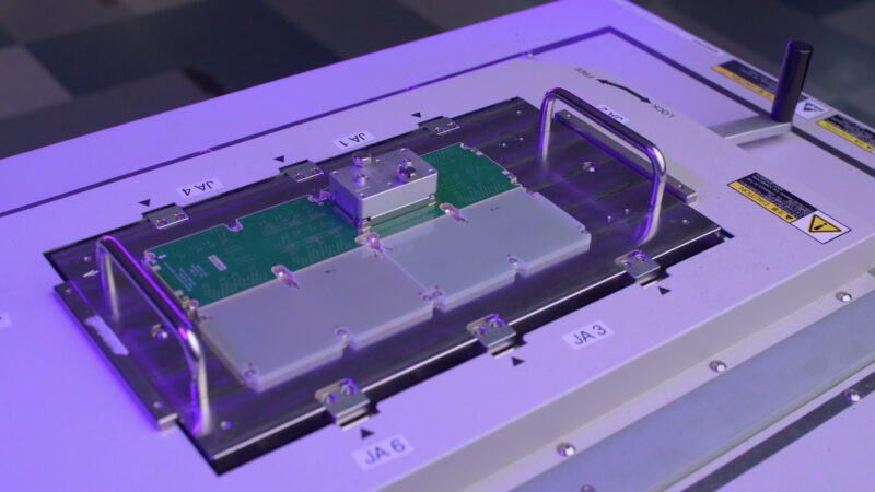
While the test setup itself is not much to look at, inside of it is a chip that, for Qualcomm, is critical to their data center plans.
Given that this was an early sample, it should be noted that HBC stack they were working with here just had 2 layers of DRAM dies. Shipping products will have 4 layers. So Qualcomm is not yet at the point where they are testing full-sized stacks.
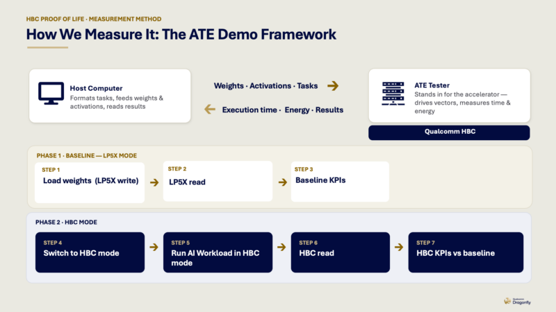
Briefly outlining their validation approach, Qualcomm tells us that they used the HBC test stack with an automated tester, which was used to measure the stack as both an LPDDR5X device and as an HBC device.
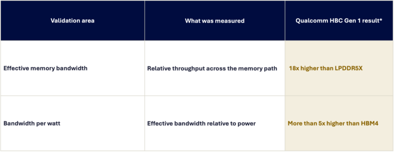
Ultimately, Qualcomm had three major findings with their successful validation testing. The first, of course, being that this worked at all, proving that it can be done. Meanwhile in regards to performance, Qualcomm measured their HBC solution as delivering more than five-times the energy efficiency (on a bandwidth-per-watt basis) than HBM4 as per its own specifications. Finally, while the company is not disclosing specific bandwidth figures, they are categorizing the measured bandwidth at 18x higher than external LPDDR5X.
The energy efficiency figure in particular is a bit short of Qualcomm’s initial projections for the technology, where they were hoping to beat HBM4 by 6x. But if this carries over to a full product, it still represents a significant improvement in efficiency.
According to Qualcomm, their validation testing also includes the thermal behaviors of the product, though the company has not gone into any further detail there. Qualcomm has had little to say on the subject so far, but thermal considerations are one of the major technical hurdles they will need to overcome, as a more active compute die as the base die in a stacked memory architecture is expected to put out more heat.
Final Words
With their initial HBC validation complete, Qualcomm is now looking at moving on to the next step of commercialization of the technology with their Dragonfly AI250 accelerator. The successor to the Dragonfly AI200 accelerator due this year, AI250 will be the first product to integrate HBC – and it will be a key part of future Qualcomm AI accelerators after that. AI250 does not have a launch date yet, but according to Qualcomm it will begin sampling in H1 of this year, which is potentially a move-up for the company’s plans following the initial announcement that sampling would take place earlier this year.
If everything pans out with HBC, the technology will not be limited to Dragonfly AI accelerators, either. Qualcomm has previously announced that they would also be bringing the technology to their consumer-focused Snapdragon products – though the company is not specifying when and what products at the time.
Ultimately, HBC is a play for energy efficiency and a lower TCO for Qualcomm. If the technology pans out, the company expects to be able to deliver AI inference accelerators that are both more energy efficient and cheaper to build than contemporary designs. Which in turn would make them cheaper to operate (and ideally, cheaper to acquire) than GPUs for large AI inference operations. We will get to see how that plays out over the coming months as Qualcomm moves towards sampling Dragonfly AI250 in the first half of next year.