
The TP-Link Omada VPN Gateway ER8411 is a neat gateway because it offers 10GbE ports. We also found that this is using a different firmware than the TP-Link BE3600 Wi-Fi 7 Portable Travel Router TL-WR3602BE we reviewed. We decided to push this and see if it could indeed push 10Gbps speeds from a $399 device. That may sound like a lot to some, but for this level of performance, it is fairly reasonable.
Here is an Amazon affiliate link to what we purchased.
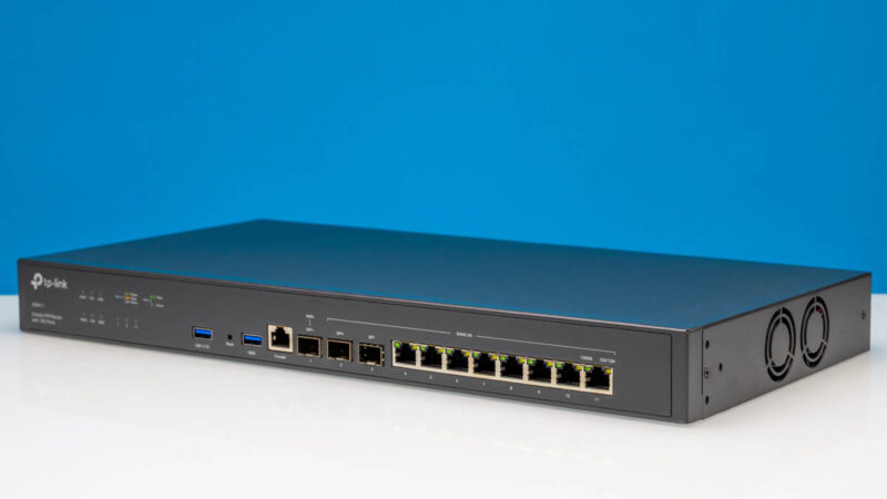
TP-Link Omada VPN Gateway ER8411 Hardware Overview
Starting with the gateway, it is a 1U chassis, and it is meant to be part of the company’s business products.
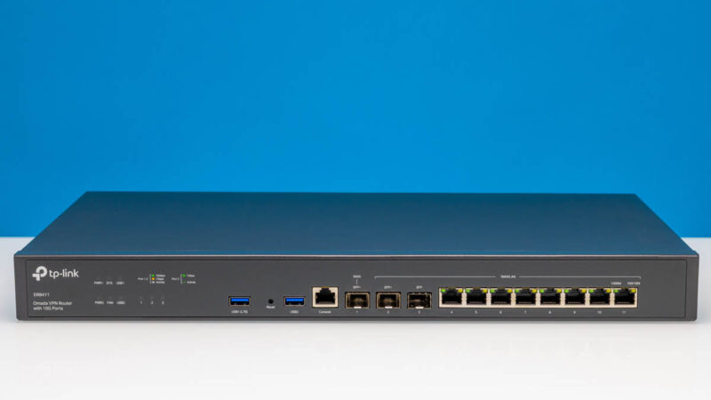
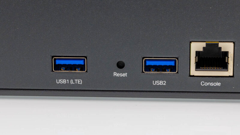
On the front, we get two USB ports, a reset button, and a console port. The USB1 is noted as a LTE one as the idea is that it can be used for a LTE connection.
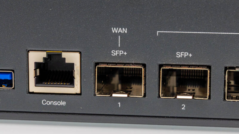
Next, we get the SFP+ WAN port as well as a SFP+ LAN port that could also be used for a WAN port. Port 3 is a SFP 1G port that can also be used for WAN or LAN.
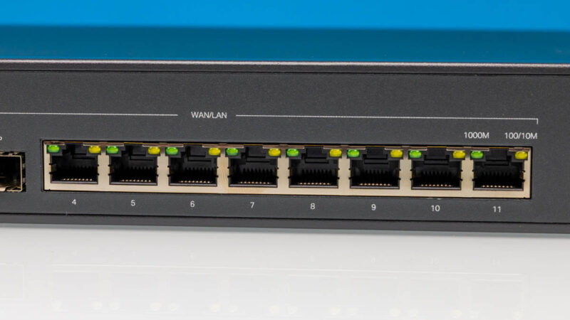
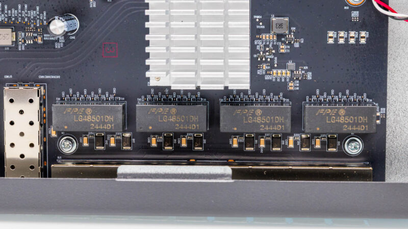
Then there are eight 1GbE ports.
Overall, this is a really nice array of ports.
On one side, we get a vent, and you can see where the rackmount ears attach. On the other side, we get fans moving air through the chassis.
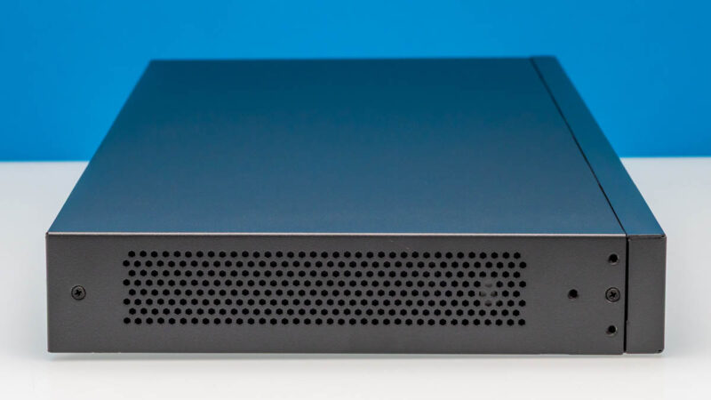
On the rear, we do not get vents, so this is a side-to-side airflow gateway.
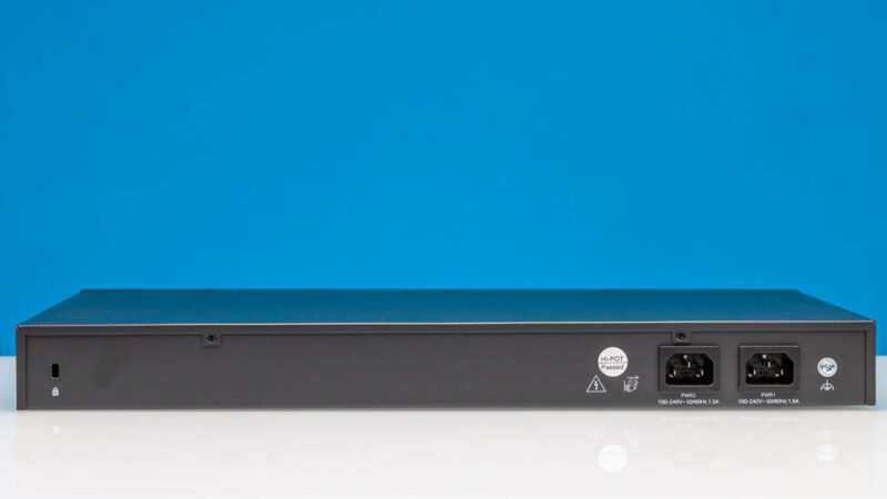
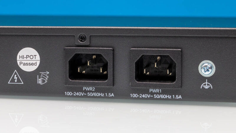
In the rear, we get two AC power inputs.
In the box, we got a console cable, two power cables, rack ears, and then rubber feet.
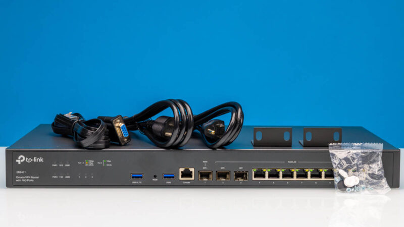
Here are the rack ears.

Inside the gateway, here is what we saw.
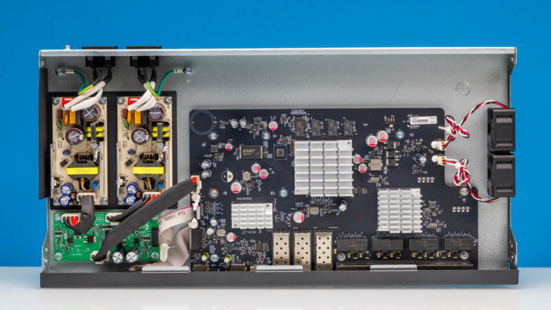
There are two internal power supplies that handle the AC to DC conversion.
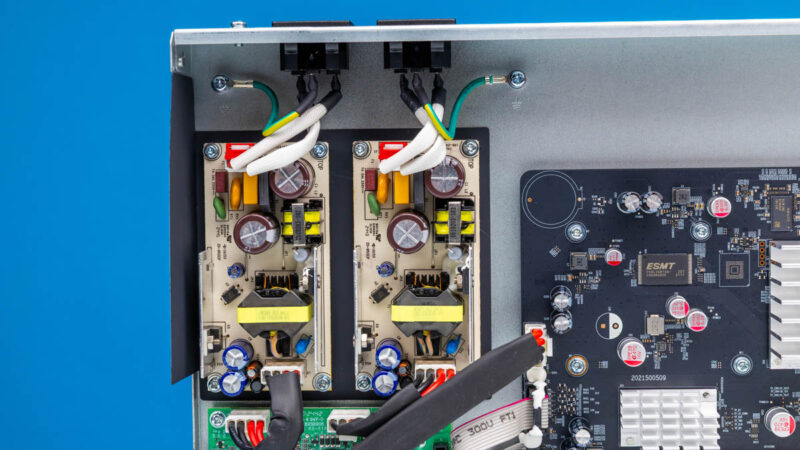
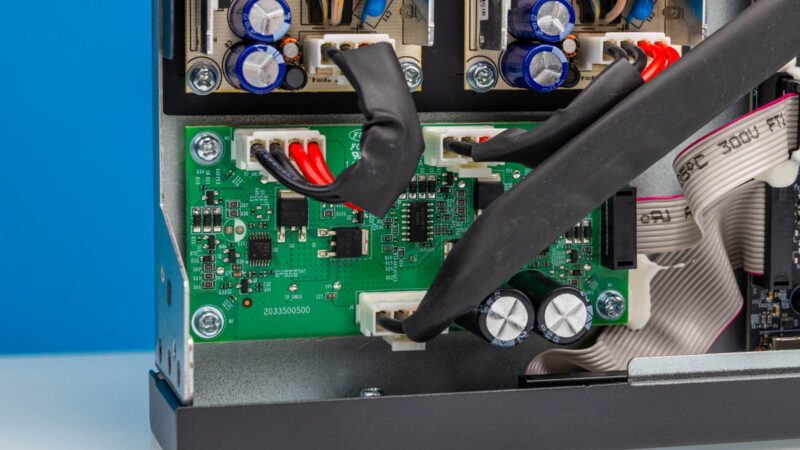
Since there are two power supplies, TP-Link is using a power distribution board to take the two power inputs and provide redundant power to the gateway.
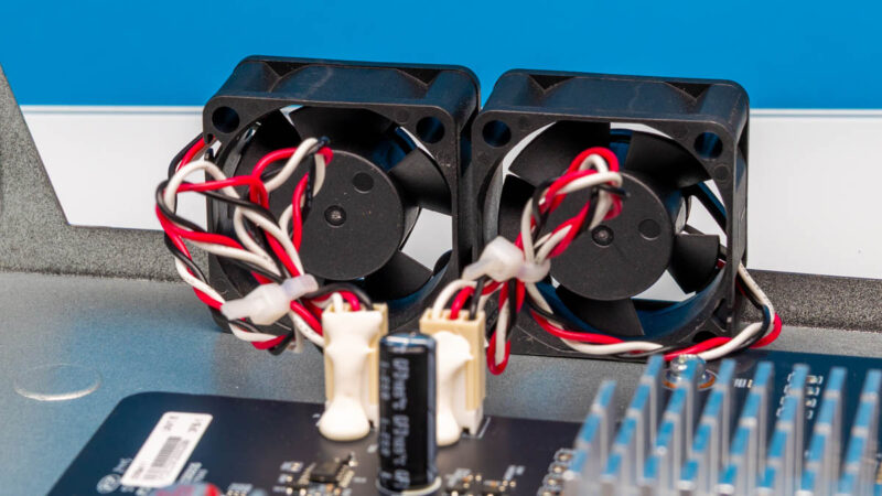
Here are the two 3-pin fans. You can see that these are glued to the board.
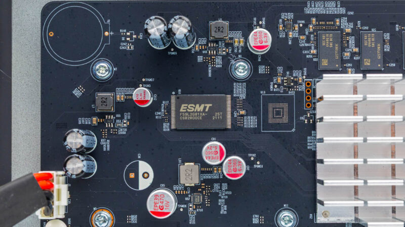
Inside, we get several heatsinks for the major chips.
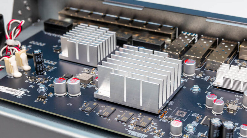
These we could not remove without damaging the unit, since they were not clipped/ screwed in. We noticed that this uses 4GB of DDR4. The main CPU is supposed to be a quad-core Arm Cortex-A72 chip.
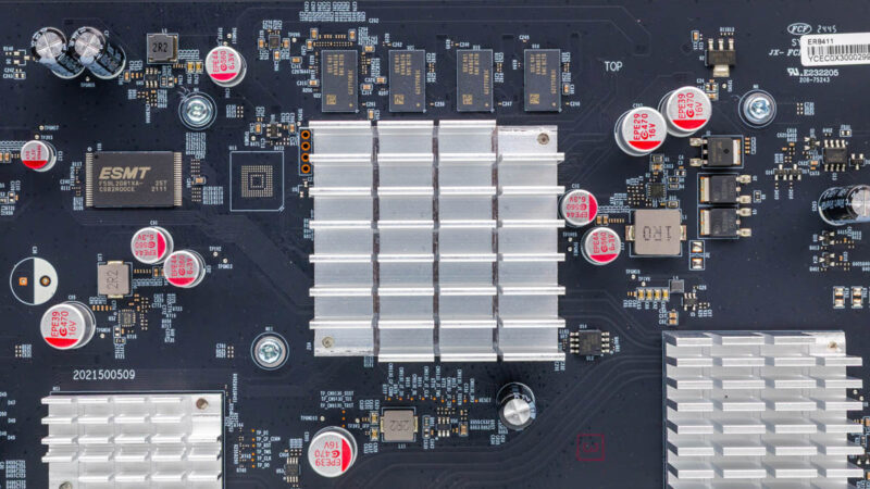
The chip to the right appears to be connected to the 1GbE ports and the LAN SFP+ port.
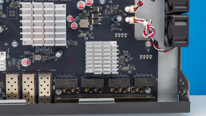
Here is another shot where you might be able to see the PCB traces.
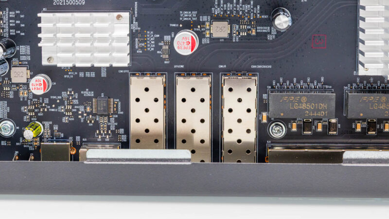
Here is behind the 1GbE ports.
Here is the ESMT NAND.
This is going to sound like an outlandish take, but given that TP-Link has some heat from the US Government, it feels like it would be better to allow folks to at least look at the components on the board. For competitors, it would be trivial to buy one of these to take apart and another to test. We are keeping ours intact since we have been using it for firewall profiling.
Next, let us get to the management.


There is a 4-pin serial header to the top left of the main chip/heatsink – be great if you were able to grab the boot log from devices and post them up so folks can see what they run ‘under the hood’
I think it is a somewhat expensive product for the feature set offered. 4 years ago I bought a Zyxel XGS1250-12. It is a very similar device (1x SFP+, 3x 10GBase-T; 8x 1G) and also a managed switch. It has been really solid and has worked well. I think it sells for around $179 these days.
Wait…
This is a “VPN Gateway”? Did I miss the part where you test VPN features? Or even describe what’s on offer?
Also I think I missed the conclusion where you said “this device is unsuited for purpose because it locks up under heavy load”.
Sorry, I should also say, it’s good that you uncovered the issue. I just feel like your reviews often leave way too many questions unanswered.
Unless one is used to the constant enthusiastic enthusiasm for new technology enthusiastically present on this website, it is easy to confuse an unfavorable review with a favourable one.
I like the enthusiasm but wonder why the network starts lagging. Does the hardware overheat under load?
I have a lesser version of the same Omada family. Same firmware and GUI. Another reviewer said its a custom GUI over OpenWRT, but I didnt see any proof of that.
As for the testing stall, the ARM Cortex was overheated and went into a deep down throttle waiting for it to recover to a normal temp.
So far it has passed all of my IPS testing, but that doesn’t rate it as impervious to attack.
I am load balancing 3 WAN’s with it, not perfect, but fine for my needs.
@Eric Olson: Its not really about the results, its the fact they have a cool new tool to play with and want to show you what it does.
This is not the Tolly Group.
Has a section about noise, not a single word about noise. VPN router review without VPN. Why do STH reviews becoming sloppier every day?
I didn’t realise these had gone up in price. I bought one at launch in November 2022, and it was $350 back then.
Most people don’t use the built-in web UI – instead, they use an Omada controller. You can get a hardware controller, or self-host it in Docker.
One thing worth noting: It took them a very long time to add an IPv6 firewall. For about a year after release, IPv6 was entirely unprotected – all inbound ports open to every device on your LAN!! Very poor security for something that’s supposed to be focused on the prosumer/SMB market. I turned off IPv6 until they finally released a firmware version with an IPv6 firewall (October 2023).
Apart from that, it’s a pretty good device and I’ve practically never had issues with it. Notably, it gets 10Gbps throughput even when using PPPoE (my ISP doesn’t, but it’s common in the UK for some reason).
Wonder how hard/cost it is to build a bare bones in China and then install your own OPNsense ?
@Tubz I suspect that that depends on your tolerance for hardware cost/power draw: x86 is going to be way easier to run OPNsense or other your-choice-of-OS on; but it’s not going to hit the same power envelope as a 4 core A-72; and unless there’s not just limited reverse engineering but proper support a weedy little ARM SoC is unlikely to manage VPN tunnels and IDS and the like at anything remotely close to wire speed since it is going to be leaning on dedicated offload for some functions.
If it’s not super mission critical; there are some great deals to be had by piggybacking on vendors who did the ‘get someone to ODM an x86’ strategy in order to get their product out the door, but only support the software for a limited period of time. I don’t know what the absolute best options in that vein are these days; but I’ve been pretty happy with the fact that a Lanner FW-7573 is quietly only $60 if it’s rebadged as a Talari e100; but there’s no way it draws less power than this thing, despite not being 10GbE.
Also of note is it looks like they were able to push it way past it’s advertised speeds. From the spec sheet:
DPI Throughput TCP: 5524 Mbps;
UDP: 3547 Mbps
IPS Throughput TCP: 4924 Mbps;
UDP: 4521 Mbps
@justsomeguy – Added a screengrab of the VPN tab. It is fair and should have been included. I think it missed the last edit of this because we are not publishing testing on it.
@Daniel – This is not the only one we have seen go up in price over the last six months.
@Eric – It is not a heat issue.
@spuwho – You are totally correct, this is not the Tolly Group.
@Multiple – On the VPN performance, that is really a can of worms. Do we just do IPSec? WireGuard? What about Fortinet and others that have their own clients? If we do all of those, what kind of traffic mixes do we push over them? What if one vendor is really good at one VPN type, but sucks at others, and we do not test that type?
Being fully transparent, I know folks want to see every feature tested. That is not really practical. Frankly, even the Tolly Group, which I have a lot of respect for and whose setup is close to what we now have, selectively tests features rather than testing every feature. They also did 2 reports between November 1, 2025 and January 31, 2026. We are doing 5+ hardware reviews per week at this point.
You may think, “if only they tested IPSec,” someone else may want to see MLPS, BGP, WireGuard, SSL VPN, in-depth QoS testing, different firewall tests, every level of firewall, and so forth. All are very valid desires. Realistically, though, testing one of these ties up test machines for, at a minimum, half a day with what we are already doing, and sometimes much longer. Nobody is remotely close to STH’s freely readable reviews in terms of breadth and depth of what we are already doing. There are two reasons for that. One, it costs too much to do even what we are doing. Two, it is an insane time sink.
We are going to keep adding testing over the next few months, but before we add a new test type, we usually back-test 24-50 devices to see if the test makes sense. Two units a day, given the timing, and the best case is that it takes 2.5-6 weeks to validate a new test. Then every review takes additional time to set up and run. If you just administer Cisco, for example, the setup steps for items are not the same on Ubiquiti, MikroTik, TP-Link, Netgear, and so forth. So doing so many vendors increases the time it takes to do them all because each needs its own procedure, down to the vendor, and often the product line. Even at the product line level from big vendors, we are finding small differences in how we have to physically set them up.
Also, that assumes everything goes right. Just yesterday, we found something failing our tests because we are pushing the gear so hard. We spent half a day validating that it indeed was an issue and giving the vendor diagnostic data on what we found. Hopefully, it makes it to a future firmware update and makes everyone’s experience better, but we are not getting paid to do this.
It is easy to say you want to see something. That is fair and good feedback. At the same time, we are spending a lot of time and money building this. We are not going to get to test every feature because there are simply too many in modern networking devices to do so if we also want to test a lot of devices.
@Patrick – That’s a very sensible answer. But I would suggest that for certain types of devices, there’s a balance point – if you can’t look at a certain minimum set of features, it might not be worth testing at all.
For example, this is a “VPN Gateway” (whatever that means) and not simply a switch. Sure, I’d want to know if the device can’t handle wire-speed switching, but if I’m buying it, it’s not so I can use it as a switch.
Your tests did do a good job in that they exposed some sort of major issue at high speeds. But if I understand correctly, it’s again using the device as a simple switch (or router?). Where’s the “VPN” part?
And yes, I get that there are lots of VPN options. Some are VERY different that others. Unless the device claims some sort of HW support for a particular type of protocol, I’d probably pick one lightweight (wireguard) and one heavyweight (IPSec? OpenVPN?) protocol, and test those.
I don’t think justsomeguy has any idea what he’s talking about. You didn’t say it was a switch. You didn’t test it as a switch. You tested it like you do gateways. I can’t imagine saying a review isn’t right if I didn’t know the difference between a switch and a gateway. Maybe he’s just trolling or an AI bot? I’d think an AI bot would know the difference if it isn’t using llama2
@justsomeguy they tested it with IDS/IPS. Not just as a switch. It would be considered a router or even a firewall (because of the IDS/IPS functions)
@MatsK… “See Figure 1”.
@J. Yes, you’re right, by the time I wrote the second reply I’d forgotten details that I should have gone back and checked. That’s my bad. My point though was that the “VPN” part of it wasn’t getting tested.
Interesting review, thank you.
What was missing here, after you found the performance drop under high load, is testing consecutively lower load levels to see if at some point the performance drop disappears. That would be helpful to establish a “functional level” of load. The way you left your finding standing out there unaddressed is somewhat unhelpful.
I hope this does lead to a firmware update. I’ve had this device for around 6 months and have not left on packet inspection because I noticed a few of these same issues.
Also some other issues with network speeds tanking with two models of their switches recently after firmware updates that only a reboot fixes. SG2210XMP-M2 and SG3428X-M2. Each has been through another newer firmware update and the problem has not been fixed.
I’ve built a few networks with omada gear because of the cloud management, and have been a bit disappointed lately waiting for things to work.
I love Omada stuff for my home… But there’s a reason I run OPNSense and then Omada gear for switches and APs…
I tried one of their 1Gbps VPN routers (ER605v2) because it had OpenWRT support, so as soon as I got it I flashed OpenWRT onto it and since then it’s been working a treat. It’s basically just a low power Linux box now that is capable of routing at wire speed, which is exactly what I was hoping for. On that one Wireguard is a little below wire speed (about 80% IIRC) but that wasn’t a problem for my use case. So if this one has the CPU power to route at 10G and it eventually gets OpenWRT support, I think I’ll probably grab one!
The Omada integration makes this interesting. I typically have Omada APs and switches, and always there is a seperately running OPNSense or OpenWRT router/firewall/VPN gateway. The question is, can the ER8411 replace an OPNSense or OpenWRT box/VM?