
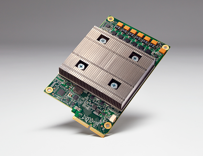
This week Google announced that it has a new Tensoflow ASIC. The ASIC is called a TPU short for Tensorflow Processing Unit. You can read details of the announcement here. Google states that the TPU offers an order of magnitude better level of performance than today’s FPGAs and GPUs that are commonly used for machine learning. Google also states that it has been using them for over a year now.
Google TPU Impact
Intel started shipping Xeon and FPGA platforms this quarter from what we have heard. Intel realized that deep learning/ machine learning require different architectures than x86 so they moved aggressively to FPGAs. At the NVIDIA’s GTC 2016 keynote, Jen-Hsun Huang clearly stated that Pascal meant that there is no need to move to FPGAs for deep learning. The fact that the TPU is already at work for a year, and Google is talking about it, also means that we would expect there to be a next-generation TPU (or two) already floating around Google.
With Microsoft, Google, Amazon, IBM and others already offering machine learning as a service, this should be a worrisome trend for those targeting deep learning with a traditional architecture. The fact that Google is going custom ASIC means that Microsoft and Amazon are going to have to choose between a traditional provider (Intel or NVIDIA), make their own custom ASIC, or both. If all of these platform as a service players go the route of custom ASICs, there is going to be a large gap between those services and off-the-shelf offerings going forward. We also know that these players get hardware well before everyone else so that means to make a TPU, Google had to look at the next 2-3 years of hardware being released and decide that it was not good enough to support Tensorflow.
As a result of this announcement, Intel, NVIDIA and to a lesser extent AMD are likely getting nervous. Here is a short list of impacts for other players:
- AMD – Their server/ desktop processor market share is extremely low. Leveraging GPU compute would have been an excellent way for them to move into a bigger market. Estimates we have heard indicate that NVIDIA has several times the market share of AMD in the data center. The TPU puts AMD no better than fourth behind NVIDA, Google and Intel, but likely a few places down the list. That is a hard road to travel if you are pushing a GPU-based alternative even with Polaris that we will see next week.
- NVIDIA – they are still selling a ton of chips. The fact that the Pascal P100 is being held for the QCT based NVIDIA DGX-1 means that there is going to be a large gap between announcement and when you can get a HP/ Dell/ Supermicro/ Lenovo compute server with the P100. With Google saying its technology is roughly 7 years ahead, and NVIDIA’s technology not yet available at retail, this gap is going to be worrisome for the company.
- Intel – With the Altera portfolio and talent Intel has the capability to bring products suited for machine learning workloads. One area Intel does decently well with is software. It does have the capability to spin up software development on a fairly large scale to support new architectures. The world is also accustomed to x86 servers which is an advantage for the players below hyper-scale.
- Xylinx – This is an example of a company that could upgrade a product like the Zynq UltraScale+ MPSoC and start to make a run at cloud machine learning applications. If ARM + FPGA becomes a preferred architecture, this could be a good move for a company like NVIDIA to make a move on (if GPUs are about to lose the machine learning space.)
- The low power ARM only architectures – we have heard of more than a few companies working on large clusters of ARMv8 chips to do machine learning. It seems like the market has moved beyond this.
Finally, Google mentioned this tidbit:
“A board with a TPU fits into a hard disk drive slot in our data center racks.”
For those that have heard me speak, I have been advocating the idea that mITX is too large for today’s SoCs for some time. One of the big reasons we are working on denser node architectures like the Supermicro MicroBlade and HP Moonshot is simply because these are the form factors that flexible next-generation platforms need to take. Using a 3.5″ drive bay form factor would be extremely compelling toward making this a reality. This is doubly so as we see 2.5″ form factor SSDs start to look bulky in comparison to their m.2 alternatives.
Discuss your thoughts in the STH forums thread here.


 ASIC being announced to the machine learning industry)